Press Releases
Flexible Hybrid Electronics: The Future of Flexible Printed Circuit Boards
Flexible hybrid electronics (FHE) is a novel approach to electronic circuit manufacturing that aims to combine the best of printed and conventional electronics. Conductive interconnects, and as many additional components as possible, are printed onto a flexible substrate, whereas the IC (integrated circuit) is produced separately using photolithography and then mounted (usually as a bare die, without packaging). This resulting hybrid of ‘printed’ and ‘placed’ functionality provides the flexibility long associated with printed electronics, but with the processing capability of an integrated circuit.
This combination of flexibility and processing capability is very desirable, since it reduces weight and enables new form factors, while maintaining desirable functionality such as data logging and Bluetooth connectivity. The technologies enabling this combination of attributes are identified and comprehensively evaluated in the new IDTechEx report: “Flexible Hybrid Electronics 2020-2030: Applications, Challenges, Innovations and Forecasts“.
FHE vs FPCB
If it’s so desirable, you may wonder why circuits with these twin capabilities haven’t been developed already. The answer is that flexible printed circuit boards (FPCBs) already provide processing capability with some flexibility. Such circuits have long been used in automotive and high value consumer electronics applications with space constraints, such as cameras. FPCBs differ from FHE circuits in that interconnects are not printed but are instead etched from a laminated copper sheet using photolithography. Surface mount components, including packaged ICs are then soldered onto the copper interconnects. The table below outlines the differences between conventional rigid PCBs, FPCBs and FHE circuits.

Benefits of FHE
So if FPCBs already exist, why bother with FHE? The simplest explanation is that by not packaging the ICs and instead using thinned silicon dies, the entire circuit can be made thinner, lighter and more flexible. Indeed, attaching packaged ICs to FPCBs normally requires a stiffener to be included to ensure that the attachment points remain secure. Such an approach introduces challenges with handling and die attach methods, which are addressed in detail in within the IDTechEx report: “Flexible Hybrid Electronics 2020-2030: Applications, Challenges, Innovations and Forecasts”.
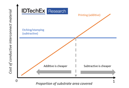
However, at IDTechEx we believe that the potential benefits of FHE go significantly beyond this, since it facilitates different manufacturing approaches and thus enables new applications. Firstly, printing rather than etching the interconnects reduces material wastage since it is additive rather than subtractive; this distinction is especially beneficial if the circuit must cover a large area with a low proportion of wiring (see schematic below). If the printing is done via digital methods, such as inkjet or aerosol, then circuit prototyping times are substantially reduced relative to conventional etching, as there is no need to design and produce masks. Such a transition to a more agile development process enables much smaller volumes of circuit boards to be economical, and even facilitates customized circuits.
From polyimide to PET
Another important distinction between FHE and FPCBs is choice of substrate materials. In FPCBs this is normally PI (polyimide), which is very temperature resistant and thus facilitates attaching components with solder and subsequent reflow heating. With flexible hybrid, the aim is to move to far cheaper substrates such as PET (polyethylene terephthalate) that have a much lower thermal budget (stabilized PET is damaged above ~150 C).
Such substrates preclude conventional solder for component attachment. The current solution is to use conductive adhesives, but these are likely to be replaced in some cases with low temperature solder as this reduces the burden on precise alignment and supports large ICs with high I/O pins. Lower processing temperatures also bring other benefits such as the ability to use thermally fragile components, along with faster manufacturing and reduced energy usage.
FHE Applications
Overall, FHE is a continuation of the path from rigid PCBs to FPCBs. For high volume manufacturing of complex flexible circuits with many SMT (surface mount technology) components, FPCBs are likely to persist in the medium term, since only minimal changes to the conventional PCB manufacturing process are required. For applications with fewer SMT components, where greater flexibility is required, or where rapid prototyping is needed, FHE is likely to dominate. Furthermore, FHE circuits can potentially be manufactured using R2R (roll-to-roll) methods due to the flexibility of thinned silicon dies and are thus well suited for very high-volume production of RFID enabled sensors, enabling smart packaging applications, for example.
A Comprehensive Overview of FHE
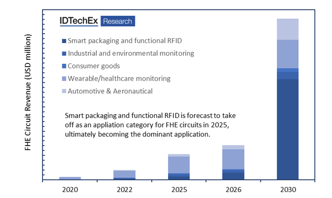
The new IDTechEx report, “Flexible Hybrid Electronics 2020-2030: Applications, Challenges, Innovations and Forecasts”, offers a comprehensive analysis of this emerging technology. At IDTechEx we have been assessing and following the printed electronic technologies and markets for well over a decade. This report is based on fresh primary research including interviews and company visits with all the key players worldwide. It identifies and examines all the key innovation trends across the material and production systems, covering attachment, substrate, and metallization materials well as production techniques including high-throughput pick-and-place and various S2S and R2R printing techniques. This report builds an application roadmap, showing how FHE will grow in complexity from simple RFID tags of today to complex flexible hybrid electronics of the future, enabling applications in smart packaging, industrial monitoring and wearable devices and more. It offers insightful analysis into application timeline, challenges, and innovation opportunities. Furthermore, it forecasts (see below) the growth of this enabling technology by both volume (left) and revenue (right). We predict that the market can exceed $3 bn by 2030. Wearable applications, particularly skin patches, are likely to dominate initially with smart packaging applications rapidly increasing from around 2025.
To find out more about printed electronics research available from IDTechEx visit www.IDTechEx.com/research/PE. Or to connect with others on this topic, IDTechEx is hosting the world’s largest Event on printed, flexible, structural & hybrid electronics: Printed Electronics USA, November 18-19 2020, Santa Clara, USA www.PrintedElectronicsUSA.com.
IDTechEx guides your strategic business decisions through its Research, Consultancy and Event products, helping you profit from emerging technologies. For more information on IDTechEx Research and Consultancy, contact research@IDTechEx.com or visit www.IDTechEx.com.
Let’s Talk About It
Creating a More Diverse and Inclusive Screen Printing Industry
LET’S TALK About It: Part 3 discusses how four screen printers have employed people with disabilities, why you should consider doing the same, the resources that are available, and more. Watch the live webinar, held August 16, moderated by Adrienne Palmer, editor-in-chief, Screen Printing magazine, with panelists Ali Banholzer, Amber Massey, Ryan Moor, and Jed Seifert. The multi-part series is hosted exclusively by ROQ.US and U.N.I.T.E Together. Let’s Talk About It: Part 1 focused on Black, female screen printers and can be watched here; Part 2 focused on the LGBTQ+ community and can be watched here.


The Profit Impact of a Market Dominating Position

Inkcups Announces New CEO and Leadership Restructure

Hope Harbor to Receive Donation from BlueCotton’s 2024 Mary Ruth King Award Recipient


Bulletins
Get the most important news and business ideas from Screen Printing magazine's news bulletin.
-

 Case Studies2 months ago
High-Density Inks Help Specialty Printing Take Center Stage
-

 Art, Ad, or Alchemy2 months ago
F&I Printing Is Everywhere!
-
 Andy MacDougall2 months ago
Functional and Industrial Printing is EVERYWHERE!
-

 Columns3 weeks ago
8 Marketing Mistakes Not to Make When Promoting Your Screen Printing Services Online
-

 Editor's Note3 weeks ago
Livin’ the High Life
-

 Marshall Atkinson3 weeks ago
How to Create a Winning Culture in Your Screen-Printing Business
-

 Thomas Trimingham2 months ago
“Magic” Marketing for Screen Printing Shops
-

 News & Trends2 months ago
What Are ZALPHAS and How Can You Serve Them in Your Print Business?